Clocking, propagation delay and the meaning of time
State requires a temporal contract
A combinational circuit computes outputs from present inputs. A sequential circuit also contains stored state. Once feedback exists, the statement “this wire is one” is incomplete unless the observation time and validity interval are specified. A voltage takes time to propagate through transistor networks and interconnect, and a storage element cannot reliably distinguish all possible input transitions at arbitrarily close instants. The synchronous design discipline arranges computation between well-defined sampling events so that a finite-state machine is a useful abstraction of that continuous physical system.
This chapter assumes CMOS switching, Boolean functions and the distinction between combinational logic and stored state. It develops timing independently of any particular commercial processor implementation. ChrisOS does not define the transistor circuit of an x86 processor. Its connection to these foundations is through architectural guarantees, timers and the explicit step model of ChrisCPU. Physical circuit timing, interrupt frequency, software scheduling and emulator instruction counts must remain distinct quantities.
Propagation and contamination delay
Consider a combinational block whose input changes at time zero. The contamination delay is a lower bound on when its output may first change. The propagation delay is an upper bound on when the output has settled to the correct value, subject to specified operating conditions and input transition assumptions. Between these limits the output may be old, transient or temporarily incorrect. Multiple paths can produce glitches even when the initial and final Boolean values are equal.
These bounds describe different hazards. The maximum delay determines whether the next sampling event occurs too early for the new result. The minimum delay determines whether new data arrives so quickly that it corrupts a value still being captured. Optimizing a circuit solely for the shortest maximum delay can therefore introduce a minimum-delay problem elsewhere. Neither bound is a universal number for a gate symbol: voltage, temperature, process variation, load capacitance and input slope affect it.
A first-order RC model explains why load matters. Charging a capacitance through an effective resistance produces an exponential approach to its final voltage. The familiar time constant R*C is a useful scale, not an exact delay for every transistor network. Logical thresholds select a point on that trajectory; fanout and long wires add capacitance and resistance. A C language expression contains no explicit capacitor, but the hardware implementing its operations remains constrained by these effects.
Edge-triggered storage and the sampling window
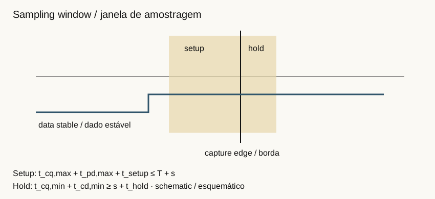
An edge-triggered register captures a logical value near its active clock edge and produces a corresponding output after a clock-to-Q delay. For reliable capture, the data input must be stable during a setup interval before the edge and a hold interval after it. These are physical constraints on the receiving storage element. They are not additional software instructions that the processor executes.
| Parameter | Meaning | Role in analysis |
|---|---|---|
t_cq,max |
Latest valid output after launch clock | Maximum-path constraint |
t_cq,min |
Earliest output change after launch clock | Minimum-path constraint |
t_pd,max |
Latest settled combinational result | Setup analysis |
t_cd,min |
Earliest combinational output change | Hold analysis |
t_setup |
Required stable interval before capture | Setup analysis |
t_hold |
Required stable interval after capture | Hold analysis |
A latch is level-sensitive: while enabled, its output can follow its input after delay. A flip-flop samples on an edge. Treating a latch as a flip-flop can accidentally permit a value to propagate through multiple stages in one clock phase. Designs using latches deliberately exploit their timing behavior; they require a corresponding phase-aware analysis. This chapter's equations use edge-triggered registers, not that more general latch model.
Deriving the setup inequality
Take two registers, a launching register and a capturing register, with combinational logic between them. Let the launch edge occur at time zero and the next capture edge at T+s, where T is the clock period and s is capture-clock arrival time minus launch-clock arrival time. Positive s means the capture clock arrives later. The latest data arrival is t_cq,max + t_pd,max. To leave the setup interval intact:
For a didactic example, let clock-to-Q be 80 ps, logic delay 600 ps, setup 70 ps and skew -30 ps. The period must be at least 780 ps before adding any uncertainty margin. That corresponds to at most approximately 1.282 GHz for this particular model. It is not a frequency specification for the ChrisOS machine or for a real CPU product. The example shows how a delay budget becomes a period constraint.
Jitter and uncertain clock arrival reduce the dependable margin. Practical analysis uses worst-case conditions, variation models and explicit uncertainty rather than a single ideal trace. A negative setup slack identifies a violated bound. Merely observing correct output in a typical-condition simulation does not prove positive slack across operating corners.
Deriving the hold inequality
The earliest new data must not disturb the value captured on the current edge. Under the same skew convention, the current capture edge is at s. The required condition is:
Increasing the period does not directly repair this inequality: it compares events associated with the same cycle boundary. Adding an appropriate delay to the short data path can repair hold, but can also worsen setup. Positive skew helps setup and hurts hold under this convention. Giving a skew number without specifying the sign convention invites an incorrect conclusion.
Suppose minimum clock-to-Q is 25 ps, minimum logic delay is 15 ps, capture skew is 30 ps and hold time is 20 ps. New data can arrive after 40 ps, while it must remain unchanged until 50 ps. There is a 10 ps hold violation. Running the clock more slowly leaves those within-edge times unchanged. This is why “lower the frequency” is not a universal cure for digital timing failures.
Metastability and clock-domain crossings
If the input changes inside the sensitive sampling window, a storage element can enter a metastable analog state. The output may take unusually long to resolve to a valid logical level. The receiving circuit cannot assume which value will be selected, and a digital zero-delay model cannot fully represent the behavior. Metastability is not an ordinary third Boolean value that application software can inspect and branch upon.
An asynchronous external signal has no guaranteed phase relationship to the destination clock. A common single-bit synchronizer samples it through a sequence of registers, allowing additional resolution time before consumers use the signal. This reduces failure probability; it does not mathematically guarantee impossibility of failure. The usual qualitative model makes reliability improve strongly with available resolution time and worsen as sampling and input-transition rates increase. Device-specific parameters are needed for an actual mean-time-between-failures estimate.
Multiple related bits cannot generally be synchronized independently and then assumed to form one coherent word. Different bits may be observed from different source updates. A handshake can hold the payload stable until acknowledgment; asynchronous FIFOs can use carefully constrained pointer encodings and domain-crossing logic. These are interface designs, not interchangeable applications of a two-register trick. For ChrisOS, software-visible completion and descriptor ownership operate above such hardware contracts; a compiler barrier is not a hardware synchronizer.
Clock frequency, latency and throughput
A clock period bounds a stage's available time. Latency counts the time from acceptance of an operation to its result. Throughput counts how frequently operations can be completed in a sustained workload. A pipeline may accept one operation per cycle while each operation requires several cycles to traverse it. Increasing pipeline depth can improve the frequency bound but add register overhead and increase latency or branch-recovery penalties.
An instruction is not necessarily one cycle. Implementations can overlap independent instructions, stall on dependencies or memory, execute internal micro-operations, and retire work under architectural rules. Consequently, counting source statements, assembly instructions or interpreter steps cannot be directly converted into elapsed seconds without a defined model. Even instructions with the same architectural effect can have very different timings across machines.
Software measurements add further questions: which clock is sampled, whether its rate is invariant, what interrupts occurred, whether the measured code was optimized away and whether memory was warm. A benchmark needs a controlled procedure and reported conditions. A theoretical operation count is valuable, but it measures a different property.
ChrisOS PIT configuration: division is not exact time
kernel/metal/pit.c defines PIT_INPUT_HZ as 1,193,182. pit_init rejects frequency zero, computes an integer divisor by PIT_INPUT_HZ / frequency_hz, and rejects divisors outside 1 through 65,535. It resets ticks, installs pit_irq for IRQ zero, writes the control value 0x36 to port 0x43, writes the divisor's low and high bytes to port 0x40, and unmasks IRQ zero through the PIC interface.
The integer division truncates. At a requested 60 Hz, the divisor is 19,886 and the nominal generated frequency is approximately 60.0001006 Hz. The nominal period is about 16.66664 ms. These are values derived from the constant and divider model, not measurements of interrupt delivery. The selected control word requests channel zero, low-byte/high-byte access, binary counting and mode three. This is a timer peripheral configuration, not a setting of the processor's instruction clock.
| Quantity | Value for the 60 Hz request | Meaning |
|---|---|---|
| Input rate in the source | 1,193,182 Hz | Divider input model |
| Integer divisor | 19,886 | Programmed count |
| Nominal output | About 60.0001006 Hz | Input rate divided by count |
ticks increment |
One per handler invocation | Delivered software event |
The handler increments ticks and calls proc_on_tick. pit_ticks returns the counter. The volatile qualifier tells the compiler that accesses have observable requirements; it does not establish a complete interprocessor synchronization protocol or convert the count into calibrated elapsed wall time. Interrupt masking, delivery latency and service behavior separate hardware events from observed handler invocations. The file's fixed work per tick includes a call into scheduler logic whose cost requires its own analysis.
ChrisCPU steps are an execution budget
chrisvm/cpu/emulator/chriscpu.c supplies a cpu_run loop bounded by max_steps and halt state. The implementation maintains cpu->steps as execution progresses. This gives the machine runner a way to limit guest work and creates an observable instruction-level progression. It does not mean that each step represents a measured host CPU cycle or a physical guest cycle.
A cycle-accurate emulator would need an additional timing model covering instruction behavior and relevant microarchitectural and device interactions. A functional interpreter can be useful without that model: it can validate architectural state transitions and execute guest code. Deterministic replay would also need controlled external inputs and timer delivery, not merely a fixed instruction budget. The current timing concepts should therefore be documented separately from any future claim of cycle accuracy.
Validation boundaries and references
Circuit timing is validated against the circuit and its physical models; interrupt behavior is validated against the platform and its delivery path; emulator budgets are validated against the interpreter state machine. A successful PIT initialization does not validate processor setup time. A passing decoder test does not establish clock accuracy. These are different evidence classes despite their shared vocabulary of cycles and ticks.
The worked inequalities above use stated artificial values and can be recomputed directly. The PIT calculation can be reproduced with integer division followed by division of the input rate by the resulting divisor. Runtime verification should additionally observe IRQ routing, interrupt masking and the scheduler callback. No physical timing measurement or guest execution is claimed by this chapter.
Primary teaching material for synchronous circuits and synchronization is available in the MIT 6.004 lecture collection. Processor-visible architectural behavior is specified separately in the Intel architecture manuals. These references supply different layers of authority; neither substitutes for reading the ChrisOS source at the recorded revision.