
Latches, flip-flops and metastability
From a Boolean function to a physical memory
A combinational function maps current input values to an output after a propagation interval. It cannot distinguish two histories that end with the same inputs. Storage requires an internal state whose future depends on its previous value. Positive feedback can provide that dependence: two inverting stages connected in a loop have stable configurations in which one node is high and the other low. The stored bit is a maintained physical condition, not a symbol floating independently of voltage, capacitance and power.
This chapter assumes the CMOS inverter and basic Boolean gates. It develops storage mechanisms before using registers as architectural objects. ChrisOS does not include a fabricated latch cell or a transistor-level simulation of its processor. The direct software connection is the architectural state represented in ChrisArchitectureState and initialized by chris_arch_reset. Physical storage theory explains the abstraction's conditions and limits; it must not be confused with the C structure implementing the emulator's state.
Two cross-coupled inverters also admit an unstable balance near their switching region. A small disturbance away from that balance can be amplified until a stable state is reached. Thus the ideal Boolean statement “the bit is zero or one” omits a physically important transient possibility. That omission is acceptable only when timing and interface design make unresolved state sufficiently unlikely at an observation boundary.
The active-high SR latch
An SR latch built from cross-coupled NOR gates has set input S and reset input R. One consistent notation is Q = NOT(R OR Qbar) and Qbar = NOT(S OR Q). The equations include feedback; they are not an acyclic evaluation order. With S = R = 0, the two stable complementary states satisfy the equations and the previous state is retained.
| S | R | Q after settling | Meaning |
|---|---|---|---|
| 0 | 0 | Previous Q | Hold |
| 1 | 0 | 1 | Set |
| 0 | 1 | 0 | Reset |
| 1 | 1 | 0, with Qbar also 0 | Forbidden complementary-state condition |
When both inputs are asserted, both NOR outputs are forced low. The problem is not that this pair of voltages is impossible; the problem is that it violates the complementary representation and does not specify which valid state should win when both inputs are released together. Unequal delays and analog noise influence the outcome. A digital truth table cannot resolve a race by declaring the simultaneous release instantaneous.
A NAND implementation normally uses active-low inputs and therefore has a different table. Transplanting the NOR table into the NAND circuit reverses the operating contract. Names such as reset_n or an overbar carry real polarity information. A hardware interface must specify both the asserted level and the allowed combinations; “set/reset latch” alone is insufficient.
Gating data instead of exposing set and reset
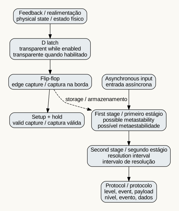
A D latch prevents the ordinary data interface from requesting set and reset simultaneously. In an ideal active-high design, S = E AND D and R = E AND NOT(D), where E is enable. When E is low both inputs are inactive, so state is held. When E is high, the latch is transparent: after propagation delay, Q follows D. The important word is transparent, because any number of input changes can pass during that open interval.
The Boolean equation Q_next = E D OR NOT(E) Q summarizes settled behavior. It does not include delays on the complementary D paths, nor does it replace cell-level timing characterization. A real circuit must ensure acceptable behavior around the closing event. Internal implementation can use transmission gates and regenerative inverters rather than a literal network of separate AND and NOR symbols.
| Enable interval | Input behavior | Observable contract |
|---|---|---|
| Closed | D changes | Q retains its earlier value |
| Open | D becomes stable | Q follows after latch propagation |
| Closing boundary | D stable across required interval | New value is retained |
| Closing boundary | D changes too close to closure | Capture is not guaranteed |
Constructing edge-triggered storage
A master-slave arrangement places two level-sensitive latches in sequence with complementary open phases. For a rising-edge device, the master can be open while the clock is low and close as it rises; the slave opens in the high phase. The master has stopped tracking D before the slave presents the captured value. Ideally the externally visible state changes at the rising boundary, even though the internal circuit uses intervals rather than a physically zero-duration event.
Real clock inversion and distribution have delay. If both latches are transparent for an unintended overlap, data may race through. If phases have excessive dead time, timing performance changes. This is why connecting arbitrary latch diagrams is not equivalent to selecting a characterized flip-flop cell. Other edge-triggered cell designs exist, and this construction is an explanatory model rather than an assertion about a particular processor.
A bank of edge-triggered elements can update multiple bits on one clock boundary. “On one boundary” remains an abstraction: clock skew and output delay vary across the bank. Downstream logic must tolerate those differences within its timing budget. Multi-bit correctness comes from the full path contract, not from assuming that every physical output changes at the exact same instant.
Setup, hold and propagation are different requirements
Setup time requires input to be stable before the capture event. Hold time requires it to remain stable afterward. Clock-to-Q delay describes the interval from capture to a valid output under specified conditions. These numbers depend on the cell, voltage, temperature, load and input transition behavior. There is no universal setup time belonging to the concept of a flip-flop.
For a launch register and a capture register, the maximum data-path delay controls whether data arrives early enough for the next capture. The minimum delay controls whether new data arrives too soon after the present capture. Lowering clock frequency can repair some maximum-delay violations but does not automatically repair hold violations, because the latter concern the same capture boundary. The separate equations and skew sign convention are developed in Clocking and timing.
Adding logic to a path might improve hold while worsening setup. A clock-tree change can alter both. Static timing analysis therefore needs minimum and maximum paths, not just the longest combinational chain. Functional Boolean simulation with ideal edges can pass while the physical design remains unsafe. The circuit and its temporal environment jointly establish correctness.
Metastability is a failure of timely resolution
An input transition near capture can leave the storage element close to its unstable balance. The eventual output may resolve to zero or one, but the resolution time is not bounded by the usual nominal clock-to-Q guarantee. The danger is a downstream consumer observing an invalid voltage or different consumers interpreting the transition differently. Metastability is not a useful third logical state for application software.
A common engineering model relates mean time between observable synchronization failures to available resolution time T_res: MTBF is proportional to exp(T_res / tau) divided by the product of destination sampling frequency and asynchronous transition frequency. The device-dependent constant tau and prefactor must come from characterization. This model explains why additional resolution time can greatly reduce risk; it cannot supply a numerical reliability guarantee without technology and environmental data.
An asynchronous signal cannot generally promise setup and hold relative to an unrelated clock. A synchronizer instead contains the risk. A first flip-flop samples the signal; a following flip-flop gives the first stage time to resolve before downstream use. Routing between the stages must leave adequate resolution time. Logic inserted between them consumes that budget. The first stage should not independently drive functional consumers that bypass the containment boundary.
A two-stage synchronizer does not solve every crossing
A stable single-bit level is the usual simple case. The destination may observe it after a variable number of cycles around the sampling boundary. The protocol must tolerate that latency. A pulse shorter than a destination sampling interval may be missed entirely even when no metastability propagates. Stretching a pulse, toggling a bit for each event, or using a request/acknowledgment protocol addresses event capture; each method has its own rate and ownership constraints.
Independently synchronizing every bit of a changing binary word does not guarantee a coherent word. During 0111 to 1000, different bits can be captured from different instants. A Gray-coded counter changes one bit per adjacent count and can help with carefully constrained pointer crossings, but it does not make unrestricted buses safe. The sending and receiving protocols still need assumptions about update rate, skew and interpretation.
For a multi-bit payload, a handshake can keep data stable while a request is synchronized. The receiver captures that stable payload and returns acknowledgment; the sender does not overwrite it until acknowledgment establishes transfer. An asynchronous FIFO extends this idea to buffered independent rates, with separate pointer ownership. The existence of storage cells alone does not establish either protocol. Memory ordering, clock-domain crossing and software locks are related coordination problems with distinct mechanisms.
Reset is a state transition with its own timing
A synchronous reset is sampled on the clock boundary and therefore requires an active clock to take effect. An asynchronous reset can force state independently of that clock, which helps establish a safe condition while clocks are stopped. Releasing an asynchronous reset near a clock event can violate recovery or removal constraints, analogous to input setup and hold. Common designs synchronize deassertion within each clock domain while permitting asynchronous assertion; this is a design pattern, not an automatic property of a reset wire.
Reset also has a logical scope. A system may reset control state without clearing every data array, provided valid bits make stale data inaccessible. Conversely, resetting a producer while a consumer retains old sequence numbers can violate a protocol. The relevant invariant is which states and ownership relationships become valid after reset, not whether every physical storage cell contains zero.
In the inspected ChrisCPU source, chris_arch_reset zeroes the provided architectural structure, sets rflags to 2 and sets CR0 bits PE and NE. This is an explicit software initialization policy. It does not describe power-on voltages, reset synchronizer circuits, or every lifecycle field in the containing CPU object. A claim about the entire machine reset would also require inspection of backend and device reset paths.
Mapping storage theory to the software model
| Layer | State representation | What establishes validity |
|---|---|---|
| Physical latch | Regenerative node voltages | Electrical operating range and timing |
| Synchronous register | Group of sampled bits | Path timing and clock/reset discipline |
| ISA register | Architecturally visible word | Instruction and exception semantics |
| ChrisCPU state | C fields in ChrisArchitectureState |
Initialization and executor update rules |
Writing a C field does not simulate feedback, metastability or clock propagation. It implements a state transition at the chosen software abstraction. Likewise, declaring a field volatile would not create a synchronizer or make a compound update atomic. Physical asynchronous inputs reach software through device and architectural interfaces; the driver must follow those interfaces rather than attempt to repair analog timing with ordinary loads.
At the hardware level, storage power includes clock distribution, internal switching and leakage. Clock enables can avoid unnecessary data updates, while proper clock-gating cells can suppress clock activity. Arbitrarily ANDing a clock with a changing software-controlled signal risks narrow pulses and extra edges. None of these transistor-level optimizations is established by the inspected ChrisCPU state definition.
Verification boundaries and further study
Truth-table checking can establish settled SR and D behavior under the allowed input combinations. Timing simulation and static analysis address path constraints. Metastability reliability needs characterized analog behavior and clock-domain-crossing review. These checks answer different questions, and a successful software build replaces none of them.
For this chapter, source inspection establishes the stated architectural reset values and the separation between an architectural structure and physical storage. No fabricated cell, analog simulator result or measured MTBF is claimed. MIT 6.004 lecture notes include primary material on storage elements and synchronization for deeper circuit study. The next conceptual step is to assemble stored bits into registers, counters and explicitly defined state transitions.