SRAM, DRAM and the memory abstraction used by ChrisOS
From a stored bit to an addressable resource
A memory cell preserves one of a set of distinguishable physical states. A memory array adds a selection mechanism so that a location can be read or written without requiring a separate external wire for each stored bit. The byte-addressable memory seen by a program is already an abstraction above cells, row decoders, sense amplifiers, controller commands, buses and address mapping. Understanding that abstraction prevents two common category errors: equating an operating-system page with a physical DRAM row, and assuming that “allocated” means “electrically initialized.”
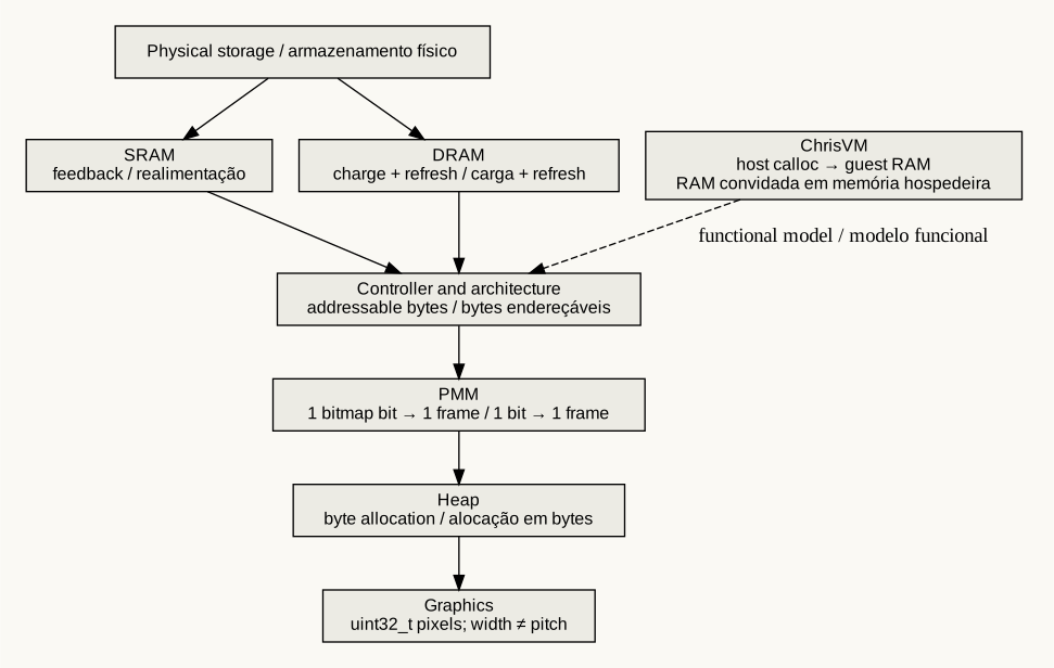
The required foundations are CMOS switching, positive feedback and sequential timing. This chapter explains ordinary SRAM and DRAM principles, then connects them to pmm.c, the graphics allocation and ChrisVM's host-backed RAM. It does not claim that ChrisOS constructs a DRAM controller or exposes the transistor geometry of the machine. Those details are supplied by the hardware platform or modeled below the guest software interface.
The six-transistor SRAM cell
A conventional six-transistor SRAM cell consists of two cross-coupled CMOS inverters and two access transistors. The inverters form a bistable feedback loop: one internal node is high while the other is low, or vice versa. The access transistors connect those nodes to a pair of bitlines when the wordline is enabled. The stored state is maintained by active feedback while power remains available, rather than by periodically reading and rewriting a small storage capacitor.
This is why the name contains “static.” It does not mean the cell uses zero power or preserves data without power. Leakage and peripheral activity remain relevant. It also does not mean that arbitrary read and write signals can be applied without timing constraints. Wordline duration, bitline development and sensing must respect the cell and array design.
During a simplified read, the bitlines are prepared and the wordline enables the selected cells. Their stored values create a small differential signal, which a sense amplifier resolves. A read must not disturb the internal state enough to flip it. During a write, the bitline drivers force a differential value strongly enough to change the selected cell. Device sizing therefore balances read stability against writability and density. The transistor count alone is not a complete description of speed, robustness or energy.
The one-transistor, one-capacitor DRAM cell
A conventional DRAM cell uses an access transistor and a storage capacitor. Enabling a wordline connects the capacitor to a bitline. Its charge is associated with a logical state under the design's sensing convention. Charge leaks over time, so information cannot be preserved indefinitely without refresh. Compared with a six-transistor cell, this organization enables high density, but requires a more involved access and restoration process.
When the cell connects to a precharged bitline, charge sharing produces a small voltage change. The sense amplifier detects that difference, drives it toward a full logical level, and restores charge to the connected cell. A read therefore participates in restoration; the isolated capacitor is not simply a permanent voltage source that can be observed without consequence. A row's sense amplifiers hold an activated row, which is commonly called the row buffer.
Refresh revisits rows within the required retention constraints. Retention varies with physical conditions, so refresh policy belongs to the device and controller contract. A kernel that allocates an ordinary physical frame normally does not refresh each byte through a software loop. The platform maintains that service underneath the memory interface. Disabling refresh would not turn DRAM into slower SRAM; it would make stored information unreliable.
| Property | Conventional SRAM | Conventional DRAM |
|---|---|---|
| Stored state | Bistable feedback | Charge on a capacitor |
| Common cell model | Six transistors | One transistor and one capacitor |
| Periodic refresh | Not required for the cell's ordinary retention | Required |
| Read mechanism | Differential bitline sensing while preserving state | Charge sharing, sensing and restoration |
| Typical architectural role | Small, fast on-chip arrays and caches | High-capacity main memory |
| Nonvolatile | No | No |
These are conventional models, not a claim that every processor array or memory product has exactly these cells. Variants trade density, ports, read stability, manufacturing constraints and power. The architectural concepts remain useful without assuming a specific manufacturer's implementation.
Rows, columns and bank state
A DRAM access is constrained by the current state of the relevant bank. An activation makes a row available to the sense amplifiers. Column operations select portions of that active row. Before a different row can be activated in the same bank, the old row must be closed and bitlines prepared under the protocol's timing constraints. A request to an already active row can therefore have a different cost from a request that changes rows.
A bank is not an operating-system process, and a row is not a virtual-memory page. The controller maps physical address bits into channels, ranks, banks, rows and columns according to the platform. Adjacent byte addresses have a defined software order, but the software-visible address alone does not reveal the complete physical geometry. Interleaving and controller scheduling can distribute traffic to exploit parallelism or satisfy timing restrictions.
This distinction explains why locality has several layers. Accessing adjacent words can improve cache-line utilization even when the programmer does not know the bank mapping. Repeatedly touching a working set larger than cache can expose main-memory bandwidth and bank behavior. A stride experiment can reveal a performance pattern, but identifying its exact hardware cause requires additional information and controlled measurement.
Decoding addresses and selecting words
An array with N independently selected locations needs enough address combinations to identify them: at least ceil(log2(N)) address bits. The data width of each selected word is separate from the number of address bits. A hypothetical 1,024-word array with 32-bit words stores 32,768 data bits and needs ten word-address bits. A byte-addressed view of its 4,096 bytes needs twelve address bits, because the two lowest bits select a byte within a word.
That example is a logical organization, not a chip pinout. A DRAM interface can multiplex portions of an address across commands. A cache additionally stores tags and state, so its physical bit count exceeds the data capacity advertised to software. Error-correction metadata and redundancy can add further storage. Capacity, bus width and pin count consequently cannot be substituted for one another in a calculation.
What a C load or store means
A C pointer denotes an address under the language implementation and execution environment. A load may be satisfied by a cache rather than by accessing a DRAM row. A store can update a cached line and become visible to other observers according to the processor's memory model and the mapping's attributes. Device memory can obey different rules from ordinary RAM. Physical cell technology alone does not specify those architectural ordering guarantees.
Coherence concerns agreement among cached copies of a location. Memory ordering concerns which relationships among accesses observers may rely on. Refresh concerns retention inside DRAM. These are different mechanisms. Adding volatile to a C pointer neither refreshes DRAM nor automatically establishes the required ordering for a device ownership handoff. ChrisOS chapters on atomics, MMIO and DMA must carry those higher-level contracts explicitly.
An uninitialized allocation is another separate issue. A memory controller can retain bits perfectly while the software allocator returns old contents from a previous owner. Initialization is a software information-flow obligation; retention is a physical storage property. Memory protection determines who may address a region, not whether its bytes have an appropriate initial value.
Physical frames in pmm.c
ChrisOS represents allocation availability with pmm_bitmap in kernel/metal/pmm.c. A physical address is converted into a page number by division by PMM_PAGE; that number selects a bitmap byte by division by eight and a bit by remainder modulo eight. bitmap_is_used tests that bit, while the set and clear helpers update it. One bit describes allocation state for an entire frame. It is not a bitmap of the electrical value of every memory bit.
For N managed frames, the allocation bitmap costs approximately N/8 bytes. If frames are 4 KiB, one bitmap byte describes 32 KiB of frame capacity. As a didactic size example, 1 GiB divided into 4 KiB frames contains 262,144 frames and needs 32,768 bitmap bytes. The actual managed range is controlled by the project's constants; this example derives the representation's cost rather than asserting a particular installed RAM size.
pmm_init initially marks the bitmap used. It then releases full frames inside boot memory-map ranges classified usable and reserves regions belonging to the platform, bootloader, executable and framebuffer classes handled in the code. Starting from unavailable state is conservative: a range omitted from the usable map is not silently donated to allocation. Reserving a framebuffer also shows why physical address space cannot be equated with a single homogeneous pool of ordinary RAM.
Alignment and partial ranges
The usable-range helper rounds the beginning up and the end down to page boundaries. Only complete frames entirely contained in the usable range are released. Conversely, the reservation helper rounds outward so that any frame touched by a reserved byte remains unavailable. These two directions are deliberately asymmetric.
For a hypothetical 4 KiB page size, a usable interval from address 0x1800 up to but excluding 0x4800 contains complete frames starting at 0x2000 and 0x3000. The partial frame at 0x1000 and the partial frame at 0x4000 must not be released based on that interval alone. A reservation covering even one byte of a frame prevents giving the entire frame to an unrelated owner. The algorithm's unit is an ownership granule, not a DRAM row boundary.
The bitmap and counters are shared metadata. The implementation has pmm_enter and pmm_leave, a spinlock, per-CPU nesting depth and saved interrupt flags. The source comments explain same-CPU recursion during a free-run callback and the need to keep an interrupt from reentering that state. This is software concurrency control over allocation metadata. It does not lock electrical cells or prevent the memory controller from servicing unrelated accesses.
A graphics buffer above the frame allocator
gfx_init obtains its backbuffer from kmalloc, using a byte size derived from width, height and four-byte pixels. The heap and physical-memory layers establish storage ownership below that request. Graphics then interprets the returned bytes as an array of uint32_t pixels. The same physical storage can therefore participate in several descriptions: cells at the device level, addresses at the architecture level, frames at the allocator level, allocations at the heap level and pixels at the graphics level.
These are compatible descriptions with different invariants. The allocator must not hand the same live allocation to two independent owners. The graphics code must stay within its allocation and distinguish width from pitch. The display path must interpret the color format correctly. Success at one level does not discharge the obligations of the others. A correct PMM bitmap cannot prevent a graphics function from calculating an out-of-bounds offset.
ChrisVM RAM is a host allocation
chris_machine_create in chrisvm/machine/machine.c allocates guest RAM with calloc, stores its size and attaches devices before creating the CPU. The configuration rejects a RAM size smaller than 2 MiB or not aligned to a 2 MiB multiple. Those checks are properties of the current machine model; they are not a statement that physical DRAM cells come in 2 MiB units.
At creation, calloc supplies zero-initialized host storage. Guest physical accesses are mediated by the machine's access functions; guest virtual accesses add guest address translation above them. The host operating system and hardware still determine how that allocation is physically backed. A guest physical address is consequently not a host physical address and cannot safely be treated as a host pointer without the emulator's translation and bounds checks.
The destructor shuts down the CPU backend and frees CPU storage, framebuffer storage, RAM and the machine. Partial creation paths release earlier allocations before returning failure. This establishes a concrete lifetime boundary for the memory model. It does not emulate DRAM refresh, row timing or retention failures. Functional RAM semantics and a physical timing model are different levels of simulation.
Failure, security and validation
Physical memory can suffer retention, signaling or cell faults. Error-correcting systems may detect or correct some error classes under their code and hardware policy. Software can also corrupt completely healthy memory through stale pointers, incorrect lengths or races. A corrupted pixel alone does not identify which layer failed. Diagnosis needs evidence that narrows the boundary: a host memory-safety test, allocator invariants, machine logs, device diagnostics or hardware error reporting.
The code paths reviewed here establish representations and lifecycle ordering, not exhaustive reliability. Reproducing the bitmap arithmetic verifies the metadata model; testing range boundaries checks its rounding invariant; inducing allocation failure checks cleanup; comparing guest reads after writes checks functional storage. None of these is a physical DRAM retention test. Similarly, a large successful allocation does not prove every physical cell was exercised or that an emulator models hardware faults.
The next architectural topics are caches and ordering; the next operating-system topics are physical allocation and virtual translation. They should be read as additional contracts above these cells. The current source evidence is limited to the declared files and revision, with platform-specific electrical organization intentionally left outside the claims about ChrisOS.